Experiment: Analog Signal Processing for Semiconductor Sensors

Analog Front-end Module
The goal of this lab is to understand typical analog signal processing steps used for read-out of semiconductor detector charge signals, plus the associated basic data acquisition and analysis methods. In this module, a single-channel analog front-end (AFE) chain made of discrete hardware components will be used to analyze the functionality of each circuit block. In particular the characterization of the noise performance and its dependence on circuit parameters will be discussed. The electrical connections to the AFE hardware allow injection of calibration charge signals, programming of circuit parameters, and the detection of hits. On the software side, scan routines will be developed to set the circuit parameters of interest and read the AFE digital output response. Basic analysis methods will be introduced to extract performance parameters such as equivalent noise charge (ENC), charge transfer gain, linearity etc. Additionally, the fast ADC can be used to record analog waveforms for further analysis.
Signal Processing Overview
A typical analog read-out chain - also called analog front-end - for a semiconductor detector consists of a charge sensitive amplifier (CSA), a pulse shaping amplifier (SHA) and digitization circuit for which the simplest implementation is a comparator (COMP), as shown in the picture below. The CSA converts the charge signal of a detector diode (or an injection circuit) to a voltage step according to the feedback capacitance \(C_f\) . The shaping amplifier (SHA) acts on the CSA output as a signal filter with a band-pass transfer function. By adjusting its band-pass center frequency the signal-to-noise ratio of the signal processing chain can be optimized. The comparator compares the output of the shaped signal with a programmable threshold. When the input signal is above the threshold, the comparator output goes high and flags a signal hit to the digital read-out logic.
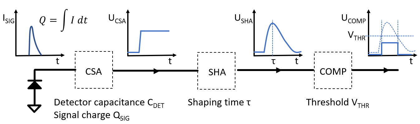
Generic read-out chain for a semiconductor detector: charge sensitive amplifier (CSA), pulse shaping amplifier (SHA), and comparator (COMP). Shown are typical signal waveforms between the blocks and the parameters that can be controlled for each block.
Circuit Implementation
The simplified schematic in the figure below shows the implementation of the signal processing chain on the AFE board.
Charge sensative amplifier
The CSA is from a low noise op-amp with a feedback loop comprising a small capacitance \(C_f\) and a large resistance \(R_f\). The feedback capacitance \(C_f\) defines the charge transfer gain while the resistance \(R_f\) creates a slow discharge of the parralel \(C_f\) capacitor and determines the DC operating point of the op-amp. The output voltage of the charge sensitive amplifier in response to an input charge Q is a step function with an amplitude given by the expression:
For calibration and characterization measurements an injection circuit is used to generate programmable charge signals. On the rising edge of the digital INJ signal a negative charge of the size \(C_{INJ}\) times the programmable voltage step amplitude VINJ is injected to the CSA input.

Simplified schematic of the analog front-end. INJ and HIT control the charge injection and digital hit readout, respectively. The SPI bus is used to program the DAC voltages VTHR and VINJ and select the shaping amplifier time constant. The full AFE schematic is found here: AFE_1.1.pdf
The shaping amplifier consists of a first-order high pass filter (HPF) and a first-order low pass filter (LPF). Therefore such a filter is also called CR-RC shaper. The high- and low-pass filter are isolated by a voltage amplifier that adds additional signal gain to the circuit. A total gain of \(g = 1000\) is achieved by using three gain stages with \(g' = 10\) each. They are located at the CSA output, between the high-pass filter and the low-pass filter (signal HPF) and at the output of the shaper (SHA), respectively. The time constants of the high- and low-pass filter are controlled by selecting the resistor values for \(R_{HP}\) and \(R_{LP}\). The control circuit sets the values such \(\tau_{SHA} = \tau_{HP} = \tau_{LP}\), i.e. the time constants for low pass filter and high pass filter are equal (\(C_{HP} = C_{LP} = const.\)). It can be shown that in this case the pulse shape in response to an input step function with the amplitude \(V_{CSA}\) is (for \(t \geq 0\))
with the peak amplitude:
where \(V_{CSA} = \frac{Q}{C_f}\). The charge sensitivity of the whole signal chain can be expressed as
and is typically given in units of \([mV/fC]\) or \([mV/electrons]\).
The final circuit block is the comparator (also called discriminator), which compares the output signal of the shaping amplifier SHA_OUT with a programmable threshold voltage VTHR. When the input signal arriving from the shaper is above the voltage threshold, the comparator will produce a ‘logic high’ output. Assuming a constant threshold, the width of the comparator output signal is a function of the signal amplitude. Some systems detect this pulse width (aka TOT, time over threshold) to get a measure of the incident charge. On our AFE board, the subsequent digital signal processing for processing the comparator output is implemented in a CPLD (Complex Programmable Logic Device). For the measurement of the time-over-threshold (TOT), this logic IC can be extended as depicted in the schematic diagram below.

Digital logic implemented in the CPLD. The SR flip-flop is set by the comparator output going high while the 8-bit counter measures the comparator pulse width (time-over-threshold), the contents of which can be read out over the SPI interface. A low state of the INJ resets HIT signal and TOT counter.
In our particular implementation of the digital signal processing, there first is a set-reset (SR) flip-flop which is asynchronously set by the rising edge of the comparator output signal COMP. The flip-flop output signal HIT stays high until it is reset by the INJ line going low. Parallel to the flip-flop, the COMP signal enables an 8-bit counter that has its output incremented (every 25 ns) by a 40 MHz clock signal CLK, thereby effectively measuring the comparator output pulse width (time-over-threshold). This TOT value can subsequently be read out via a SPI interface implemented in the CPLD logic (CS_B, SCLK and MISO). Finally, a high to low transition from INJ resets the TOT counter.
The electrical interface to control the AFE consists of
An SPI interface controlling
the shaping amplifiers time constants by selecting filter resistor values via a multiplexer
a digital to analog converter (DAC) which sets the injection step voltage VINJ and the comparator threshold VTHR
the read-out of the TOT counter value via the CPLD SPI interface (if implemented)
And two GPIO signals
INJ output signal (GPIO4, from Rpi to AFE module) that triggers the injection signal and resets the comparator latch
HIT input signal (GPIO5, from AFE module to Rpi) for reading the digital hit output
A typical charge injection and digital read-out cycle would look like this:
Set INJ to ‘0’ to reset the HIT output of the digital logic (and TOT counter, if implemented).
Set threshold, injection level (and shaping constant) as required.
Set INJ to ‘1’ to trigger the injection of a negative charge signal. Add a small delay (~100 us) to allow the signal to propagate through the circuit.
Check the state of the HIT signal. If a high level of the HIT is detected store the information. If the (optional) TOT signal is to be acquired, wait approx. another 100 µs (the maximum detectable pulse width) to allow the counter to stop before being read-out.
Set INJ back to low to reset the HIT signal and the TOT counter.
Since the CSA also responds to positive charge injection (INJ going low), wait for ~ 200 µs to allow the circuit to settle before triggering the next injection.
Data Acquisition and Analysis Methods
An important performance metric of a signal processing circuit is its signal-to-noise ratio (SNR), which is directly related to the efficiency and accuracy of the detection process. A noiseless system would generate a comparator hit signal with 100 % probability if the signal is above threshold and always detect no hit if the signal is below threshold. In the presence of noise, however, the step-like response function of the comparator hit probability as a function of the difference between signal and threshold is smeared out. The following figure shows the comparator response probability of a real system and an ideal system. When the injected charge is equal to the comparator threshold \(Q_{INJ} = Q_{THR}\), the hit probability is 50% in both cases. In a noiseless system the hit probability immediately goes to 0 % (100 %) for lower (higher) charge. The noise smooths out this transition region. Actually the knowledge of the slope at the 50 % probability mark allows the calculation of the noise i.e. the noise is proportional to the inverse slope. Mathematically, the response curve is given by a Gaussian error-function (also known as “s-curve”). It is the convolution of a step-function (the ideal comparator response) with a Gaussian probability distribution (representing the noise).
The normalized error function describes the response probability of the comparator as a function of the signal charge in the presence of noise. The mathematical expression is given by the following equation:
where \(\mu\) is the mean value and \(\sigma\) is the standard deviation of the Gaussian distribution and \(erf\) is the error function:
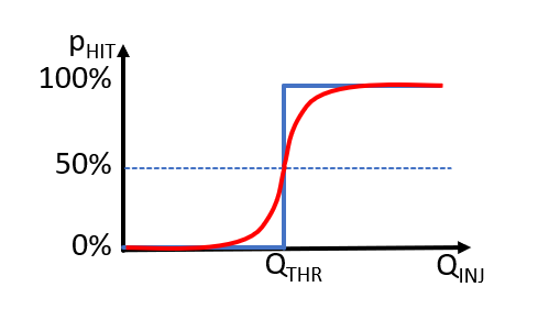
Response probability of the comparator as a function of the signal charge. The ideal system (noiseless, blue curve) exhibits a step function, while noise (red curve) will smear-out the transition. That results in a Gaussian error-function, which fitted parameters define the threshold (50 % transition point) and the noise (slope of the curve) of the system.
The measurement of an s-curve is based on a nested loop of injection/read-out cycles. The following steps need to be implemented in a scan routine (also called threshold scan):
Set threshold and shaping time constant to the desired values.
Outer loop: Define a range of injection voltage values (i.e. injection DAC values) to scan. The injection range must cover the chosen threshold, i.e. the transition from zero hits to 100 % hits must occur within the scan range.
Inner loop: For each charge value repeat the injection and read-out cycle (see above) a number of times (typical 100) and count the number of detected comparator signals in relation to the total number of injections.
Finally plot the hit probability data as a function of the injection voltage.
The dataset for the injection voltage scan will represent an s-curve that allows the extraction of the threshold and the noise. For a quantitative evaluation of the s-curve the injection voltage (i.e. DAC setting) has to be converted to the equivalent injection charge \(Q_{INJ}\).
with \(k = 0.1\) for the attenuation of the resistive divider in front of the injection switch and \(C_{INJ} = 0.1 pF\) for the injection capacitance which converts the voltage step into a charge.
or
with the elementary charge \(q = 1.602 \cdot 10^{-19} C\).
The threshold voltage of the comparator corresponds to the peak amplitude of the shaper for 50 % hit probability. Therefore, the threshold can be expressed in units of input charge dividing the threshold voltage by the charge sensitivity of the system \(g_{q}\) as calculated above.
Both voltages VTHR and VINJ are generated by a 12-bit digital to analog converter (DAC). The maximum output voltage of the DAC is 2048 mV. This corresponds to a LSB step size of 0.5 mV for VTHR and 0.05 mV for VINJ, respectively, taking into account the attenuation of an additional resistive divider in front of the injection capacitor. With this information the threshold and the injected charge can be converted from DAC register units to charge units (electrons). With this ideal equations and ideal gain constants, the shift along the x-axis for s-curves measured at different threshold settings would be equal to the difference of the injected charge, i.e. if the threshold would be changed by a certain amount of charge (threshold voltage DAC change) the 50 % point of the s-curve would shift by the same amount of injected charge (i.e injection voltage DAC value). However, as the later experiments will show, the gain constants are not ideal and the conversion of the x-axis of the s-curve to charge units has to be calibrated by measurement. The dominant error contributions come from the fact that the sensitive components (i.e. the injection and the feed back capacitance) are very small and therefore the effective capacitance is affected by the parasitic capacitance of the PCB. What can be measured with the injection circuit is the ration of the injection gain and the charge sensitivity of the system. An absolute calibration can only be achieved with a detector diode exposed to a monochromatic X-ray source (radioactive isotope), which would generate a known amount of charge in the sensor, avoiding the uncertainties in the size of the injection capacitance \(C_{INJ}\).
Exercises
The pre-lab exercises (Exercise 0) are questions which must be answered before coming to the lab, with the method of your choosing, although Latex may be preferable to avoid duplicating effort with the report.
The in-lab exercises (Exercises 1-3) are grouped into three section. In the first part the basic functionality of the analog front-end is tested. This is accomplished by implementing a script to enable the charge injection and to observe waveforms of the charge sensitive amplifier, shaper, and comparator with an external oscilloscope and/or the fast ADC on the Raspberry Pi base board. In the second part methods to extract analog performance parameters from the digital hit information will be developed. Finally, the full analog signal processing chain will be characterized as a function of shaping time and detector capacitance.
Exercise 0: Pre-lab questions
Please answer the following questions before lab:
The injection circuit generates a charge signal of the size \(C_{inj} \cdot V_{inj}\). What is the charge in femto-Coulombs generated by a voltage step of 100 mV with \(C_{inj} = 0.1 pF\)? What is the charge step size for \(V_{inj} = 0.05 mV\)? (This voltage step corresponds to the effective LSB size of the injection voltage DAC.) What is the expression to convert these charge values in Coulombs to units of the elementary charge (electrons)?
An ideal charge sensitive amplifier generates a step-like voltage output waveform in response to an instantaneous charge signal at the input. What is the CSA output step amplitude for an input charge of 1 fC, assuming the feedback capacitance is \(C_{f}=1 pF\) ? If charge sensitivity is defined as the output amplitude per input charge, what is its unit?
A shaping amplifier responds with a characteristic output pulse to a step-like input waveform. Assuming a step input and a CR-RC (high-pass + low-pass filter) with equal time constants, at what time does the output pulse peak, and what is the amplitude of that peak?
To a first order, what is the charge sensitivity of our analog front-end chain (CSA + SHA)? Put another way, what is the pulse peak amplitude in mV at the shaper output, per fC (or electron) charge at the CSA input? (Note: Use the effective feedback capacitance value \(C_{f} = 1.39 pf\) for your calculation.)
Following the CSA and SHA, a discriminator with programmable threshold voltage is used to detect the pulse. This discriminator is essentially a comparator with one input voltage set via a DAC with an LSB size of 0.5 mV. What is the equivalent of this LSB size in units of fC or electrons ? Hint: Use the “transfer function” calculated above which relates charge input to voltage output (sensitivity).
The threshold of the comparator should be set in a way that the noise is suppressed and only the signals are detected. What would happen if the threshold was too low, what would happen if it was too high? How could the terms purity and efficiency of the detection process be defined in this context? What happens if baseline and signal fluctuations are getting too close to each other?
The term ‘equivalent-noise-charge’ (ENC) expresses the voltage noise in a measured output signal, in terms of the equivalent input charge that would produce it. Given the charge sensitivity we calculated above, what would be the ENC for a measured 10mV output noise amplitude?
How are the discriminating comparator’s Gaussian distribution and the error-function related? How can one extract the width (sigma) and the mean (lambda) of the underlying Gaussian distribution from a measured error function? How is the noise calculated from the slope of the error function at the 50 % point?
Draw a sketch of an amplitude histogram of an ideal noise-free system. It consist of two delta-like peaks: one for the baseline and one for the signal amplitude produced by a constant input charge. In a real system, however, noise is overlaying the ideal signals, leading to fluctuations of the baseline and signal amplitudes. Modify the amplitude histogram to reflect these fluctuations (assume a Gaussian distribution of the noise).
Draw an optimum threshold in your amplitude histogram.
The term ‘equivalent-noise-charge’ (ENC) represents the quantity of electrons at the input of an ideal (i.e. noise-free) signal chain that would produce the same amplitude at the output as the noise alone would in a real system. What is the ENC value for a noise amplitude of 10 mV given the charge sensitivity calculated above?
Exercise 1. Characterizing an analog front-end
The first set of exercises is intended to familiarize you with the analog front-end hardware and the control software. The goal is to observe the different signals of the analog front-end chain (CSA, SHA, COMP) and to understand the effect of the different circuit parameters on the signal shape. To monitor the signal waveform, connect an oscilloscope to the LEMO socket OUTPUT. Use the jumper bank in front of the LEMO socket to select the signal to be monitored manually (CSA, HPF, SHA, COMP) or use the setting MUX to select the signal to be monitored via your program code with the SPI interface. Note: As mentioned in the circuit description above, the shaper circuit adds a total gain of 1000 to the CSA output signal. This gain is split in three gain stages with G=10 that are distributed along the signal chain in front of the CSA, the HPF, and the SHA output, respectively. The CSA output is amplified by 10, the HPF accumulated amplification is 100 and the shaper output SHA finally accumulates the total gain of 1000.
Once you are familiar with the signal generation and monitoring, switch from the external oscilloscope to the fast ADC on the Raspberry Pi base board to record and save the waveform data for further analysis. Connect the monitor signal to the ADC input on the base board and set the gain jumper to 1. The trigger for the waveform acquisition should be derived from the charge injection signal. To select this trigger source set the TRG jumper to GPIO4. The fast ADC is controlled by a Python script osc.py which can be found in the folder FAST_ADC. The script needs root privileges to access the interface to the fast ADC and thus has to be started by calling sudo -E python osc.py. A simple command line interface of the osc.py tool will allow you to set the horizontal resolution and the saving of acquired waveform data to file (csv) or to save a waveform image (png).
After reading the above, answer the following questions in your lab report:
A negative charge is injected with the rising edge of the INJ signal, which will generate a positive amplitude at the CSA, HPF, and SHA outputs. What happens at the falling edge of the INJ signal? What happens if the time delay between the rising and the falling injection signal is too short? What circuit parameters do you have to take into account to estimate the maximum injection frequency?
Implement a routine to continuously inject charge pulses into the CSA and observe the different signals (CSA, high-pass filter HPF, shaper SHA, and comparator COMP) while varying the injected charge amplitude, shaper time constants, and comparator threshold. To get a reasonable comparator response, the threshold needs to be set in a range between the baseline of the signal and the pulse peak amplitude (remember the LSB step size of the threshold DAC is 0.5 mV). Advanced: You could use threading to change configuration parameters to avoid needing to stop, modify and restart your injecting loop script (see
threads.pyas an example for using threads in Python).Make a small table of DAC values for VINJ vs. peak voltages measured after the shaping amplifier. Also calculate which VTHR DAC value would be just able to still discriminate this signal. The table will be useful for setting reasonable parameters in later exercises.
Select an injection amplitude that is well within the dynamic range of the system (i.e. no amplitude clipping but also well above the noise floor). Sample the SHA output with the fast ADC and save the waveforms to file for each time constant setting of the shaper. Write a script that can read and plot the saved waveform data (CSV format). Add a fitting function to the pulse shape (assume an ideal CR-RC pulse shape with equivalent time constants for low and high pass filter) and extract the peaking time and peak amplitude for each shaper setting. Does the peak amplitude change with the peaking time? Give possible explanations. Optional: Implement a fitting function for the shaper pulse with independent time constants for high and low pass filter.
Advanced task: (Not mandatory, only attempt if time permits) Calculate and plot the time-over-threshold as a function of the ratio of CR-RC shaper peak amplitude and threshold voltage. You can do that either by inverting the mathematical expression for the shaper pulse waveform (-> Lambert W function) or by implementing a function representing the shaper pulse waveform in Python and numerically evaluating TOT width for a range of amplitude values at a fixed threshold. Note: this function will be useful to fit measured pulse waveforms (see the later exercises). What is the relation between the TOT and the injected charge? What is the effect of the shaping time constant on the TOT? Assume the TOT counter has a resolution of 25 ns and a maximum count of 255. What is the maximum detectable TOT width in this case? Assume the maximum amplitude to threshold ratio is 10. What is the maximum shaping time constant that can be used in this case?
Exercise 2. Characterizating a digital read-out
In this section, we will understand the behavior of the logic which quantizers and records the hit information in a digital manner. Please answer the following questions in your report:
First, select the comparator output with the monitor multiplexer. Set a threshold at half of the shaper peak amplitude (the Vthr DAC gain is 0.5 mV/DAC step). Observe the pulse width of the comparator output (time-over-threshold, TOT) for different injection amplitudes with an oscilloscope or the
osc.pyapplication. What relation between TOT and injected charge would you expect? Measure (by hand) the average TOT value for 5-10 different input charge values. An automated TOT measurement using the hit signal to start and stop a digital timer will be implemented later with the FPGA lab module.Implement a scan routine to measure the s-curve of the system. The s-curve is obtained by measuring the hit probability as a function of the injected charge. The charge is varied by changing the injection voltage. The hit probability is calculated by counting the number of hits (using the comparator output pulse) for a given charge step in relation to the total number of injections. Be sure to convert the x-axis of the s-curve from DAC units to charge units (in electrons) Note: The effective value of the feedback capacitance is \(C_{f}^{eff} = 1.39 pF\) due to the parasitic capacitance of the PCB traces and the feedback resistor which add to the nominal value \(C_{f} = 1.0 pF\)
Use the measured s-curve to extract the threshold (50 % value) and the noise (proportional to 1/slope at the 50 % point). Repeat for different threshold settings. Does the change of the measured threshold (in injection charge units) correspond to the change of the threshold DAC setting in threshold charge units (both in electrons) as you have calculated above? How large is the deviation?
Exercise 3. Noise performance of complete
Finally, we will understand the performance of the system in aggregate. Noise plays a critical role, as you have read in the pre-lab questions:
Acquire s-curves for different shaping time constants. What is the effect of the shaping time on the noise? (Do not connect a sensor diode to the CSA during this step, as we just want characterize the AFE circuit in isolation.)
Now connect a sensor diode to the CSA and apply 20 V bias voltage. Repeat the s-curves measurements. What happens if you lower the bias voltage? What is the effect of the detector capacitance on the noise performance?
Connect various test capacitors instead of the sensor diode and plot the noise vs. input capacitance. Repeat the measurements for different shaping time constants.